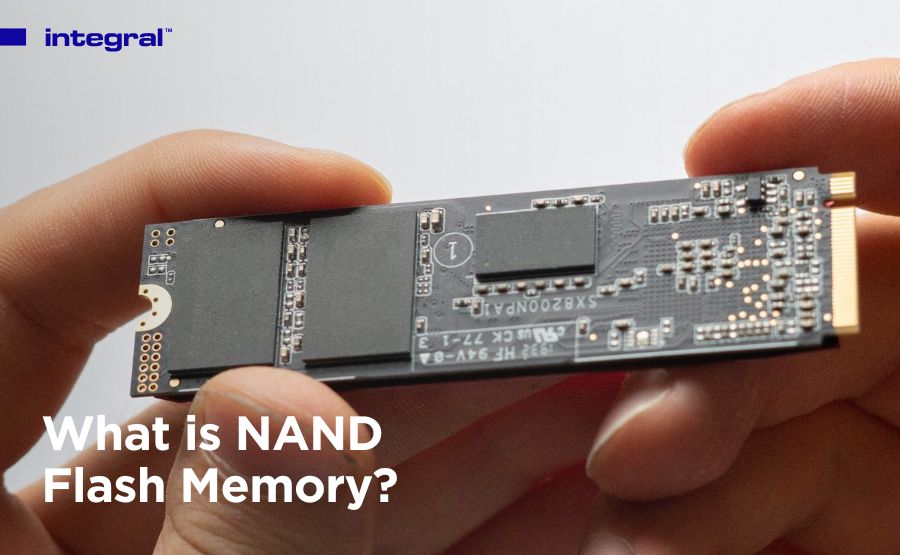
NAND flash memory is a type of non-volatile storage technology meaning that it can store data without continuous power input. Endeavouring to minimise cost per bit while maximising chip capacity, NAND flash memory has quickly become the go-to storage solution for devices such as MP3 players, digital cameras, SSDs and USB flash drives, excelling in scenarios where large files are frequently saved and erased.
How Does NAND Flash Work?
At its core, NAND flash memory employs electric circuits to store data in blocks, utilising the capabilities of metal-oxide semiconductors. Commonly known as the floating-gate transistor (FGT), this component of flash memory mirrors NAND logic gates, enabling data storage and retrieval.
NAND flash is created from a circuit grid of individual
cells. At the intersection of each cell with another, there are two transistors
(the floating gate and the control gate) separated by a thin layer of
metal-oxide semiconductor material. These gates work together to manage data
flow, with a voltage charge sent to the control gate to program a cell.
Each cell of NAND flash can either store or erase an electric charge. As long as the gates are linked the cell is erased (or does not hold charge) indicated as a binary 1. If voltage is applied, the charge of the semiconductor layer is altered blocking the connection between the two gates in a process known as Fowler-Nordheim tunnelling, a phenomenon that involves the movement of electrons across the oxide layer. This process effectively switches the cells value to binary 0 and the cell holds a charge programming it. Applying a higher voltage charge will then return the cell to a 1 by erasing the data and reconnecting the two gates.

Memory Wear Out
The process of charging and erasing data within the NAND flash memory cells, while integral to its functioning, introduces an issue known as “memory wear-out.” This captures the inherent limitation of NAND flash technology – a finite lifespan marked by the wear and tear endured by individual flash cells during their operational life.
As electrons undergo the process of tunnelling, moving across the metal-oxide layer during data programming and erasure, the semiconductor materials within the floating gate undergo stress and strain. This repetitive action takes a toll on the structural integrity of the semiconductor components, gradually causing physical degradation and a slow deterioration of the flash cell’s ability to reliably retain and transmit data.
The problem of memory wear-out is inherent to the workings of NAND flash memory so manufacturers employ various strategies to mitigate its impact. Advanced error correction techniques, wear levelling algorithms and sophisticated management of program and erase cycles are implemented to enhance the overall longevity and reliability of NAND flash devices.
End-users, especially in applications where frequent write and erase operations are commonplace, need to be aware of this characteristic. However, it’s important to note that for most consumer applications, the typical lifespan of NAND flash memory far exceeds the expected duration of usage, ensuring reliable performance over an extended period.
Types of NAND Flash
Diverse types of NAND flash storage are manufactured— including SLC (single-level cells), MLC (multi-level cells), TLC (triple-level cells), QLC (quad-level cells), and 3D NAND — catering to varying needs by adjusting the number of bits per cell. SLC, storing one bit per cell, boasts high endurance but comes at a premium. Multi-level cells store two bits per cell, but what they gain in capacity they lose in durability as write and erase cycles occur twice as many times as SLC. This compromise between longevity and storage capacity persists across the various tiers of layered NAND flash storage.

The majority of NAND flash storage devices employ 2D or planar configurations for their cells, where the cells are positioned horizontally alongside one another. 3D NAND stacks cells vertically enhancing capacity and allowing the chips to remain compact whilst increasing storage. However, creating 3D NAND chips is a costly and complicated process.
NAND flash memory continues to evolve to meet the escalating demands of modern data storage. Its resilience, speed, and cost-effectiveness position it as a cornerstone in the dynamic landscape of memory storage technologies.